A nanomaterial is usually defined as a substance with dimensions in the 1 – 100 nm.
In this size regime many aspects of the properties are affected, including electronic and surface characteristics. From a purely geometric perspective, the key change is the surface area to volume ratio is drastically perturbed. Most nanomaterials of interest are either metals or semiconductors.
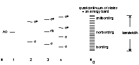
Bonding in metals and semiconductors is based on covalent principles of orbital overlap but extended over volumes larger than molecular sizes.
The construction of these orbitals can be viewed in a step-wise fashion:
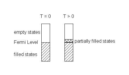
In metals the orbitals are not filled but there is a temperature dependence of the orbital occupation.
The distribution of orbitals form waves and so it is common to represent the metallic orbitals as waves described by a wave vector, k, and an energy.
The relationship between the molecular orbital space (known as real space) and wave space (known as reciprocal space or phase space) is the Bloch Equation:
Ψk = ∑nN e2πi k· rn φn
where the sum runs from n = 0 to n = N and
Ψk is the wavefunction in reciprocal space
n is the counter of the orbital locations in real space
N is the number of sites in the sample (typically Avogadro's Number)
i = √–1
k is the wavenumber vector
rn is the real space vector translating from the origin to the cell number n
φn is the basis atomic or molecular orbital at site n in real space
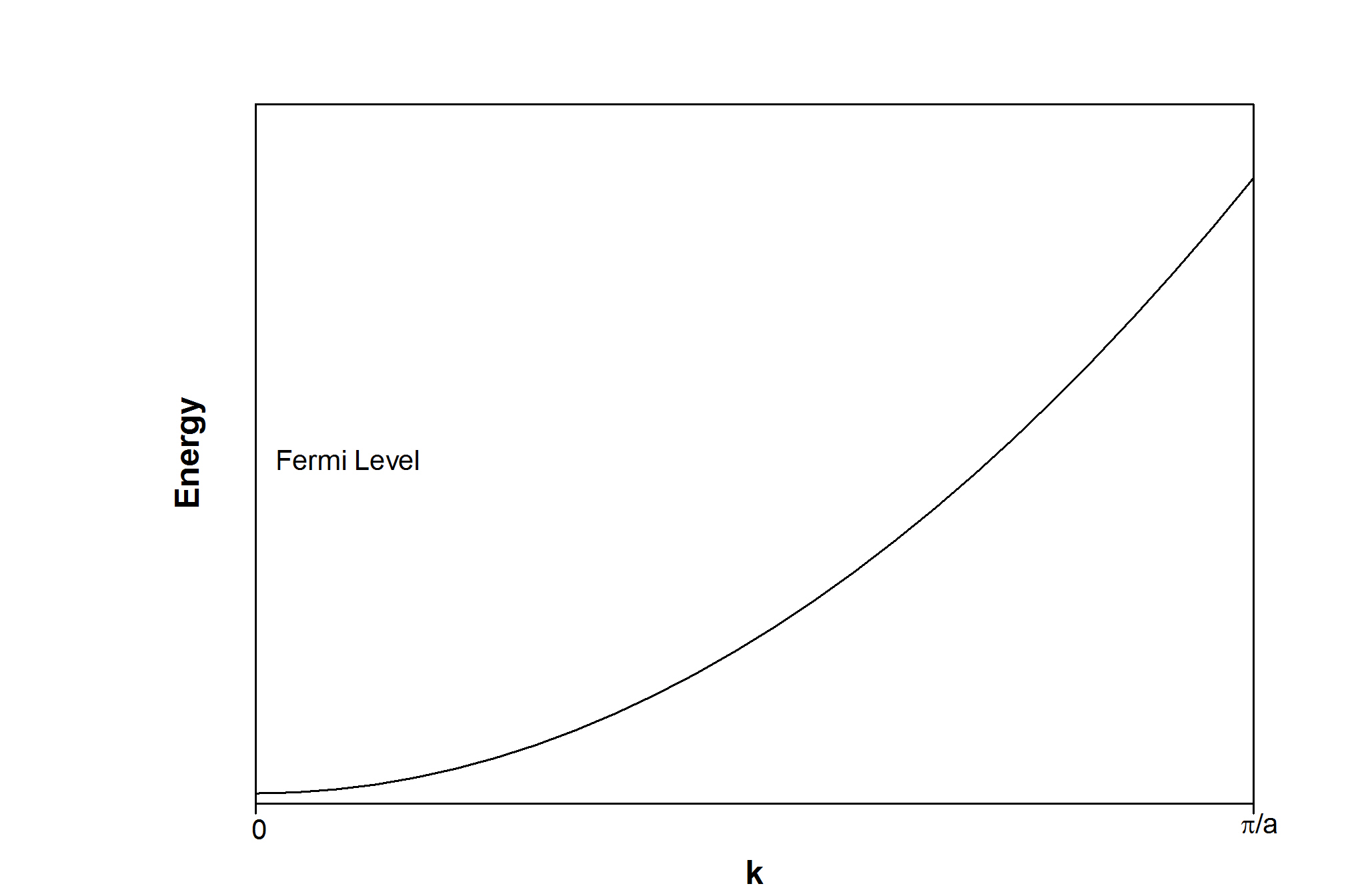
Thus, the energy levels of metals are typically graphed as a function of wavenumber. For a free electron in one-dimension with a unit cell length = a, this looks like:
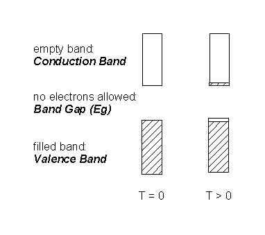
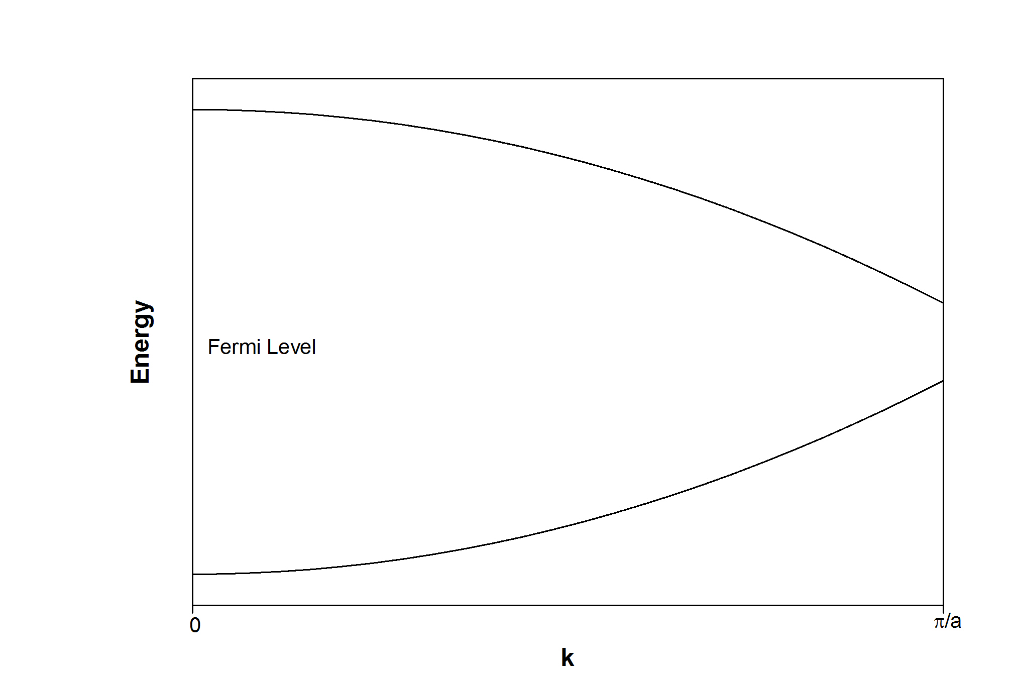
For semiconductors a gap opens up at the Fermi Level. In real space:
In reciprocal space:
One of the biggest and obvious influences that particle size has is on the optical properties of nanoparticles, which can be tuned depending on the particle size.
In bulk metals the interaction of the electric field of light with the electrons on the surface of the metal induces a surface wave called a plasmon. In most metals, since the electrons in bands can respond readily to the applied electric field, the resonance frequency is very high so absorption is in the UV regions, so most metals appear white or silver to the eye.
An common exception to this is gold, which is yellow in the bulk.
In nanoparticles, the small size of the particle restricts the wavelength (equivalently, the wavenumber) of the surface plasmon. Thus, the absorption and color of metal nanoparticles can be controlled by changing the size and geometry of the metal nanoparticle. Then, for example, gold nanoparticles can range in color from yellow to purple to red.
One application of using metal nanoparticles in spectroscopy is for SERS (Surface Enhanced Raman Scattering). SERS relies on electric field enhancements created by metal plasmons. These enhancements have been shown to be greats at corners and step edges one the metal because the electric field created is larger. Nanoparticles are ideal because there are more corners and edges per volume than in a bulk metal.
Semiconductor nanoparticles are often called quantum dots. These are usually binary or ternary compounds.
The absorption spectroscopy in semiconductors is controlled by the band gap. The band gap in nanoparticles varies with particle size because the number of orbitals involved in the Bloch Equation are limited (N does not approach Avogadro's number).
This is referred to as quantum confinement.
Semiconductor nanoparticles also are fluorescent with high quantum yields, which allows them to be used light emitting diodes
Nanoparticles are often effective catalysts because of the high surface area. In addition, the small particle size leads to many edges and corners where catalysis often occurs.
With the discovery ~30 years ago that C has more than the traditional two phases (graphite and diamond), a number of interesting C only structures have been intensely studied.
C60, buckminsterfullerene (Ih symmetry), is probably at the border of molecular vs. nanoparticle.
This was followed by the discovery of Carbon Nanotubes. These come in two varieties: single-walled (SWNT) and multiwalled (MWNT). Depending on the details of the structure, carbon nanotubes can be either metallic or semiconducting.
Graphene: this is a single layer of graphite and is currently under intense study.