
Chemistry 401
Metals
Physical Properties: hard, ductile, malleable, electrically conductive, thermally conductive, high mp, high bp
What type of bonding leads to this?
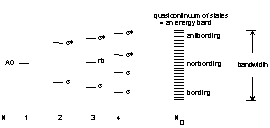
Metals are crystalline (i.e., atoms are regularly spaced in three dimensions) but have no ions, so consider covalent bonding in a crystalline lattice built up a little at a time.
In metals the bands are not completely filled; since there are more bonding states filled than antibonding there is a net bond energy that can be quite large - hence high mp and bp The metal molecular orbitals are extended over many atoms (hundreds or thousands).
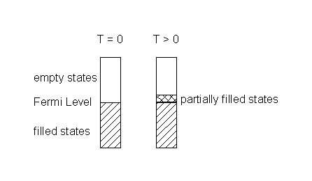
The energy of the highest occupied molecular orbital in a metal is called the Fermi Level:
Electrical Conductivity
Adding heat or electrical energy: the electrons can accommodate additional energy because the empty excited states are at very low energy; further, the input energy can be distributed over the entire lattice because the wavefunctions are delocalized over large numbers of atoms. Thus, metals have high electrical and thermal conductivities.
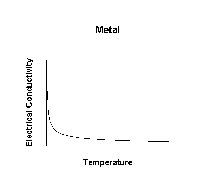
Why is there any electrical resistance?
Defects in the lattice disrupt the delocalization of wavefunctions. 'Defects' can be created by vibrations. Since the number of vibrations that are active depends on temperature, thus the resistivity must also depend on temperature. In general, conductivity = σ = neμ, where n is the number of charge carriers, e is the electronic charge, and μ is the mobility.
Semiconductors
Properties: not as hard as metals, lower mp and bp but still solids, not ductile or malleable, poor electrical conductors - in many ways like a bad metal!
How do we explain this in terms of bonding?
Band theory but with more basis orbitals : require two bands, one filled and one empty
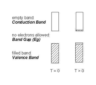
If the band gap is large enough, the material is an insulator because no metal-like properties arise from a filled band
If the band gap is on the order of thermal energies (small), then excitations of electrons from the valence band into the conduction band occurs
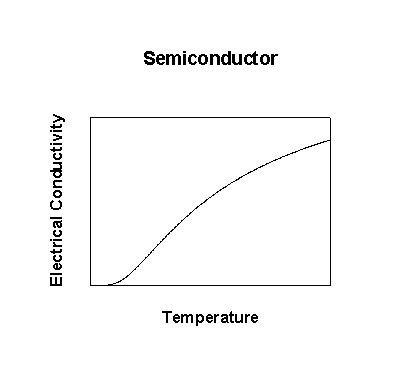
σ = neμ where n = eEg/RT (Boltzmann population of the conduction band)
μ has the same properties as in a metal but the Boltzmann term dominates so the conductivity of a semiconductor increases with increasing temperature
Doping of Semiconductors
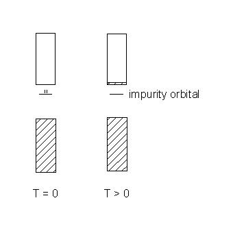
Case 1 : the impurity has a filled orbital in the semiconductor band gap
Charge carries are created thermally (T > 0) by excitation from the filled impurity orbital into the conduction band. The population of the valence band is undisturbed; since it is filled, no charge can be transported through the valence band. The dopant is a species with more valence electrons than the semiconductor.
This is an n-type semiconductor.
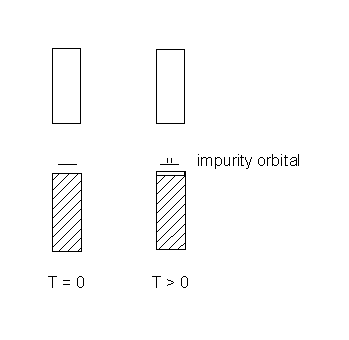
Case 2. the impurity has an empty orbital in the band gap
At T > 0, the valence band is depopulated thermally creating charge carriers in the valence band (the electrons in the impurity orbital are not mobile, they are too far apart). The dopant must have fewer valence electrons than the semiconductor.
This is a p-type semiconductor
Semiconductor devices
Bonding properties at interfaces are the key to semiconductor device applications:
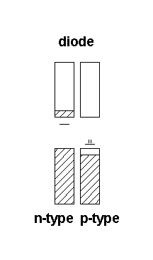
Electrons flow in one direction - from n-type to p-type
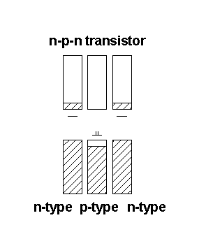
Under depicted conditions there is no electron flow – the electrons get trapped in the p-type device. Adding a potential to the p-type semiconductor, effectively populating the conduction band, can turn on electron flow.